Toggling an LED using GDB (on STM32)
Today we will be looking at how you can toggle an LED on a microcontroller board using GDB. At the end we should have a practical understanding of memory mapped IO. We won’t be writing any Assembly or C code but knowledge of pointers is beneficial.
We will start by learning some fundamentals so anyone with a basic understanding of computer architecture can follow along, if you would like to skip fundamentals click here
Some Fundamentals
LED & GPIO

An LED is a semiconductor that emits light when current passes through them, like the ones in the image above.
To control the current in our LED, we need to connect it to a GPIO pin on our microcontroller. We would then use code to control the state of the GPIO pin.
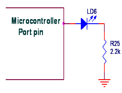
A GPIO (general purpose input/output) is just a pin on a microchip that can be user configured & controlled at runtime, typically using code. You can for example set a pin as input, attach it to a sensor like a digital thermometer & read temperature data from it or set it as output and use it to turn an LED on or off or even use it to control an AC appliance via a relay.
Target Hardware
You can follow along with any microcontroller that uses memory mapped IO by referencing its datasheet. I’ll be setting up an emulation lab using Qemu so anyone without the hardware can also follow along, maybe even with an actual visual of the LED blinking, but thats for a future article
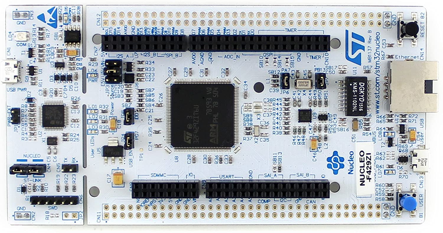
We will be using this NUCLEO Development Board. It has an STM32F429Zi on it, this is the microcontroller. You can also see the GPIO pins we mentioned earlier exposed on this board, allowing it to be connected to external devices like sensors.
The microcontoller is basically the CPU, it has a Cortex-M4 Core, 2MB of ROM/flash memory, 256KB of RAM and peripherals. Some of these peripherals are for communicating via various protocols e.g serial and some are for general purposes usage, like the GPIOs.
We will be using the following documentations / reference manuals:
The board has 3 on board LEDs that are connected to the MCU GPIO pins. We will blinking one of this LEDs.
Memory mapped IO
Memory mapped IO is a method for performing input/output operations between CPU/MCU & peripherals in the device/computer. An example of a I/O device / peripheral could be a GPIO pin, Serial/UART port, a USB printer etc.
I/O devices are mapped into the system memory map along with RAM and ROM. To access an I/O device, e.g an LED, simply read or write to their mapped addresses using the normal memory access instructions.
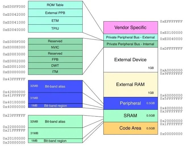
The image above shows the memory map of a Cortex-M4 device. When an address is accessed by the MCU, it may refer to a portion of RAM, e.g 0x20000000 in this case, or it can instead refer to memory of the I/O device, e.g 0x40000000, this is because the memory and registers of the I/O devices are mapped to address values.
If you want to learn more about memory mapped IO you can take a look at this Liveoverflow memory mapped IO video.
Getting a GDB shell
To debug the microcontroller using GDB we need a debugger/programmer board like the ST-Link, luckily our nucleo board comes with an on-board ST-LINK/V2-1, which can even be used to debug/program other cortex-M microcontrollers.
We will also need to install:
- GNU ARM Toolchain to get GDB
- stlink for programming and debugging STM32 devices and boards
After connecting the debugger to your PC via USB, you can start a GDB server by running st-util, to be safe I made sure to first erase the MCU’s flash with st-flash erase.
$ st-util
st-util 1.6.0
2022-02-06T19:31:25 INFO common.c: Loading device parameters....
2022-02-06T19:31:25 INFO common.c: Device connected is: F42x and F43x device, id 0x20036419
2022-02-06T19:31:25 INFO common.c: SRAM size: 0x40000 bytes (256 KiB), Flash: 0x200000 bytes (2048 KiB) in pages of 16384 bytes
2022-02-06T19:31:25 INFO gdb-server.c: Chip ID is 00000419, Core ID is  2ba01477.
2022-02-06T19:31:25 INFO gdb-server.c: Listening at *:4242...
GDB server is now listening on port 4242, you can now use GDB to interact with the baord:
$ arm-none-eabi-gdb
GNU gdb (GNU Arm Embedded Toolchain 9-2020-q2-update) 8.3.1.20191211-git
Copyright (C) 2019 Free Software Foundation, Inc.

For help, type "help".
Type "apropos word" to search for commands related to "word".
(gdb)
From GDB, connect to the server using:
(gdb) target extended localhost:4242
Remote debugging using localhost:4242
warning: No executable has been specified and target does not support
determining executable automatically.  Try using the "file" command.
0x08000398 in ?? ()
We get a warning that an executable wasn’t specified but thats fine since we dont plan on using any firmware image. At this stage we can start manipulating the system memory from GDB. For more info you can look at STLink Manual
If you need a refresher on GDB, you can check out:
Toggling the LED
Which LED?
First we need to figure out how the on-board LEDs are connected to the MCU GPIO. From the board’s reference manual, section 6.5, we can see we have 3 usable LED pins.
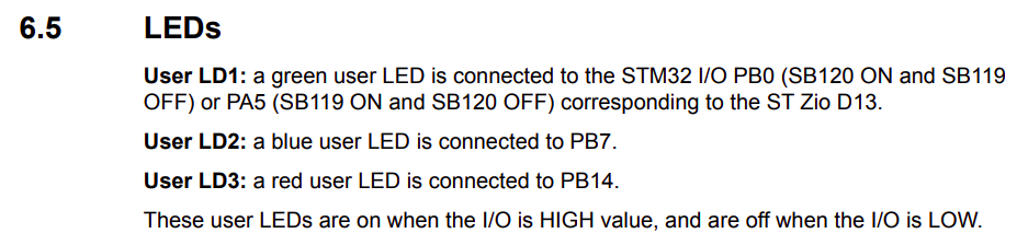
We will be toggling the Blue LED2 which is connected to GPIO port B Pin 7, PB7 in short.
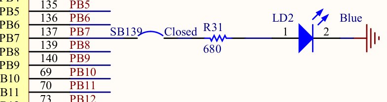
We will need to do the following to toggle the blue LED connected to PB7:
- Enable
GPIOBperipheral clock. - Set GPIOB pin 7 as output.
- Toggle GPIOB7
Turning On the GPIO Clock
Before using any peripheral, we first need to enable its clock. Inside the MCU, just like in our PC, there’s an oscillator providing a clock signal that is used to synchronise diferrent parts of the chip. On Cortex-M, by default a peripheral’s clock is usually off to prevent it from consuming power when its unused, this technique is called Clock gating.
To use GPIOB7 pin, we need to set up the clock for the GPIOB port, enabling it to drive the port, otherwise the port is off and won’t respond to any reads or write to its address space.
On STM32 this is accomplished by setting the appropriate bits in the Reset & Clock Control registers. RCC is the engine that controls the clock for all the domains of the microcontroller, since the RCC is also a memory mapped peripheral, we can configure it by writing to its memory mapped registers. We will refer to the STM32F4x Reference Manual section 2.3 to know the where RCC registers are mapped in system memory.
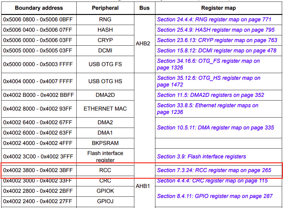
From the image above we can see its mapped to address 0x40023800. Next, lets look at the RCC register map, in section 7.3.24, this is wehere we are going to find out exactly which RCC register we need to write to in order to turn GPIOB clock on.
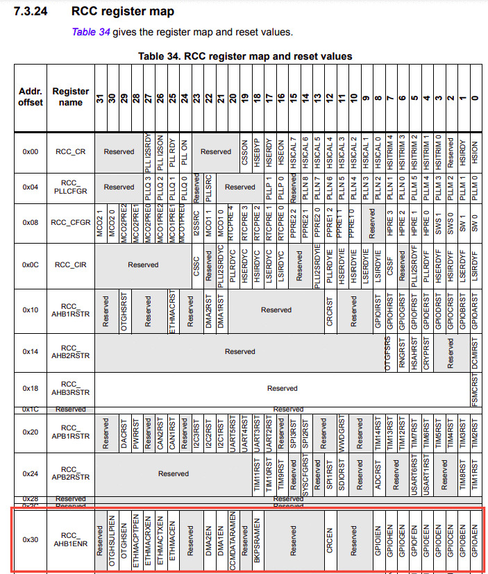
The first column in this table shows the address offset from the base address we noted earlier, 0x40023800. The numbers from 31 to 0 show the bits of the 32-bit registers. At offset 0x30 we can see register RCC_AHB1ENR, its used to configure clocks of peripherals connected to the AHB1 (advance high-speed) peripheral bus, one of these peripherals happen to be GPIOB. If we look closely, we can see the bit field GPIOBEN for enabling GPIOB’s clock. More details on RCC_AHB1ENR register is available on section 6.3.10
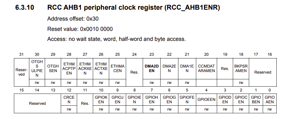
In RCC_AHB1ENR register, we find the bit positions to control the clock for various GPIO ports from GPIOA to GPIOK, DMA, Ethernet, OTG etc. Setting a corresponding bit as 1 enables the clock, clearing it to 0 disables it. We need to set bit GPIOBEN, this bit controls the clock gating for Port B. If set, the module receives a clock and functions. Otherwise, the module is unclocked and disabled.
Lets first see the initial value in this register,
#display value in hex format
(gdb) x /x 0x40023830
0x40023830:	0x00100000
#display value in binary format
(gdb) x /t 0x40023830
0x40023830:	00000000000100000000000000000000
(gdb)
Its seems like the 21st bit is set on system reset, from the doc this is the DMA1EN bit. We don’t care about that now so let’s set the GPIOBEN, which is the second bit.
(gdb) set *((unsigned int*)0x40023830) |= 0x2
(gdb) x /x 0x40023830
0x40023830:	0x00100002
(gdb) x /t 0x40023830
0x40023830:	00000000000100000000000000000010
(gdb)
We converted the address of RCC_AHB1ENR (0x40023800 + 0x30) to an unsigned pointer *((unsigned int*)0x40023830) then set GPIOBEN bit using bitwise |= 0x2, next we can confirm that the bit is set by reading the value on the register x /x 0x40023830 which we can see the GPIOBEN bit has been set 00000000000100000000000000000010.
Configuring GPIOB7 as output
Now that we have the peripherals clock enabled, we need to set GPIOB7 as output. Just like with RCC we can look at the base address for GPIOB then see which of its registers we need to write to. From the memory map shown earlier (section 2.3 ) GPIOB is mapped to 0x40020400.
Seems like the register we want is GPIOx_MODER, used to configure the I/O direction mode, essentially as output, input or other alternate functions like using a GPIO pin for serial communication(UART etc). The documentation says the reset value for port B is 0x00000280, lets confirm this in GDB. There is no offset this time as the MODER register is the first GPIO register.
(gdb) x /x 0x40020400
0x40020400:	0x00000280
(gdb) x /t 0x40020400
0x40020400:	00000000000000000000001010000000
(gdb)
Seems good, my guess is because pin 4 & 5 are used for alternate functionalities like debugging(NRST) & ethernet.
To set GPIOB7 as output, we need to change the two-bit field MODER7 to be 01, output mode, we can use bitwise OR again to set the MODER7 bits at position 14.
(gdb) set *((unsigned int*)0x40020400) |= (0b01 << 14)
(gdb) x /t 0x40020400
0x40020400:	00000000000000000100001010000000
(gdb) x /x 0x40020400
0x40020400:	0x00004280
(gdb)
A read on the memory address x /t 0x40020400 confirms that the MODER7 bit field is set 00000000000000000100001010000000.
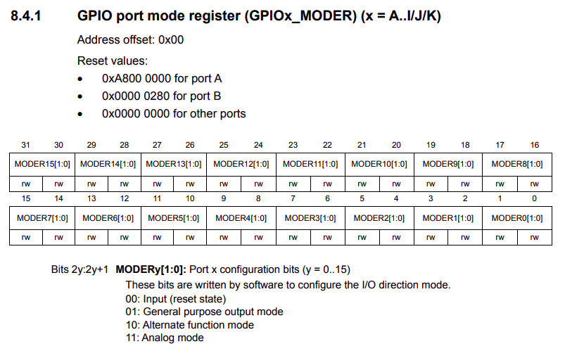
Toggling the LED
Finally, its time to toggle the LED, looking at the GPIO documentation, it tells us that there is an output data register GPIOx_ODR.
The documentation warns us that the access to this register is not atomic, but thats not an issue since we are not doing any context switching. In a future post I will explain how you can avoid GPIO concurrency issues using bit banding or the GPIOx_BSRR register.
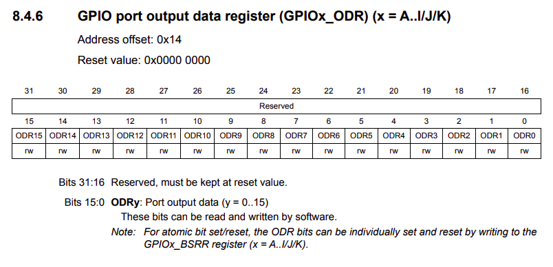
To set GPIOB7 as high we will write 1 to bit 7, writing 0 to bit 7 sets it to low, lets do this in GDB, the GPIOx_ODR register is at offset 0x14, so its address will be 0x40020414 for our case
(gdb) set *((unsigned int*)0x40020414) |= (0x1 << 7)
To turn off the LED we clear bit 7 in ODR register, using bitwise &= ~(0x1 << 7)
(gdb) set *((unsigned int*)0x40020414) &= ~(0x1 << 7)
That’s it for today.
Resources
- GDB Documentation To get started on using GDB
- Memory Map and I/O Registers Liveoverflow CTF writeup Memory mapped IO